GaN is the chemical symbol for gallium nitride, which is an III-V semiconductor material commonly referred to as a 'wide bandgap' (WBG) material, because it has a relatively high energy requirement (compared to silicon or Si) to knock an atom’s electron from a valence band (e.g. – insulator) to a conduction band (e.g. – conductor).
semiconducting devices
When it comes to an electronically-controlled switch, users want a material that has a high breakdown electric field (e.g. – blocking voltage) when off and very low-resistance conduction channels when on, which is why WBG materials make great semiconducting devices. Some other WBG semiconductors heard of are silicon carbide (SiC), gallium arsenide (GaAs), or aluminum nitride (AlN).
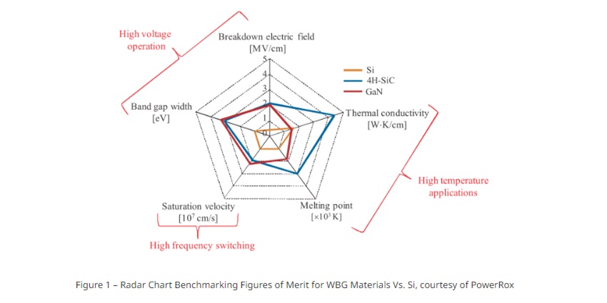
GaN also has some other interesting properties that make it attractive for several applications. Its electron mobility and melting point enable high-current channels and higher temperature (or increased reliability at relatively same or lower temperatures), respectively.
lower gate charge
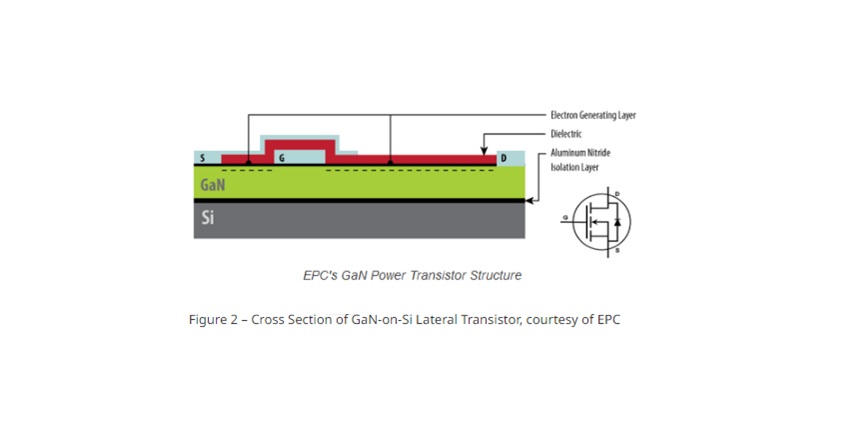
When fabricated into transistors, the resulting devices can have lower gate charge and equivalent on-state channel resistance (RDS_ON) than Si-based metal–oxide–semiconductor field-effect transistors (MOSFET). Though there are many types of GaN-based switches, let’s focus on the GaN high-electron-mobility transistor (HEMT as an example of one kind, (its structure is shown in Figure 2).
With the gate activated, current flows very quickly through the shallow GaN layer in what is sometimes called a two-dimensional electron “gas” (2DEG), as represented by the dotted line in the figure.
Applications
While GaN has been used for many decades in light-emitting diodes (LED) and RF applications, it has only been in the last decade or so that its usage in switch applications, such as switch-mode power supplies and inverters, has become more common.
The attractive properties described above enable power supplies designed with GaN switches to address many of the key size, weight, and power factors (a.k.a. – SWaP factors) that tend to be the critical drivers of practically any power solution design.
Lower efficiency
Lower RDS_ON and gate transition times help to reduce conduction and switching losses
Lower RDS_ON and gate transition times help to reduce conduction and switching losses (respectively), which can lead to overall increased efficiency of the power train.
These characteristics offer another bonus characteristic of enabling control of the switches with a lower duty cycle (D), which enables higher, direct conversion ratios that were impractical with MOSFETs (e.g. – direct 48 V to 1 V conversion).
When Fast is Too Fast
WBG switches can be fast, really fast. They get about as close as you can to the kind of ideal (e.g. – zero transition time) switches, first, learn about in textbooks.
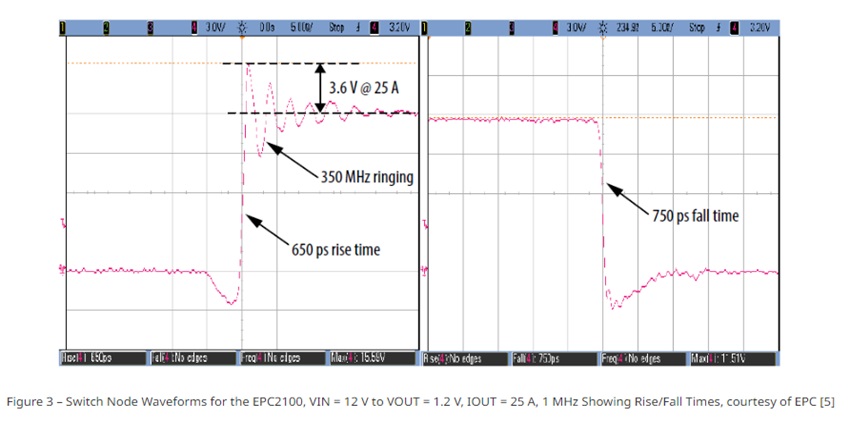
These speedy transitions are due to the very low gate charge and very high electron mobility properties of materials like GaN. Turn-on and turn-off transitions can occur in <1 nanosecond (1 ns = 10-9 seconds) even in some fairly high-power applications.
scope BW
These transitions are so fast that most engineers trying to measure these transitions on their boards are likely not even using an oscilloscope with the appropriate bandwidth (BW) to sufficiently capture (e.g. – see Nyquist–Shannon Sampling Theorem).
If needing to properly measure and characterize a signal with transitions in the nanoseconds, then scope BW needs to be in the GHz range. These kinds of scopes are generally very expensive and usually designed for high-speed data applications rather than power stage analysis.
negative ramifications
WBG components are NOT drop-in replacements for their Si contemporaries
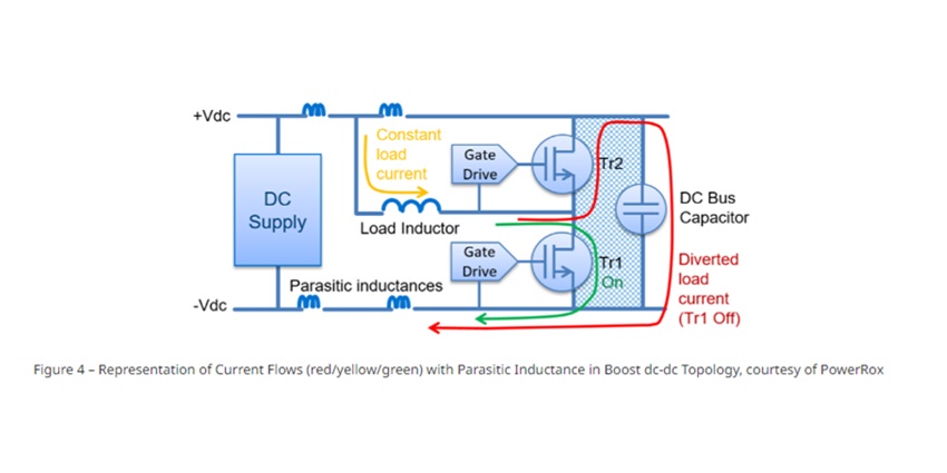
The negative ramifications of these extremely fast switch node transition rates are increased electromagnetic interference (EMI) and overshoot/oscillation events, both of which are attributed to undesired energy dumps, or more specifically improper flow of high-energy transition currents to ground, into parasitic inductance or equivalent series inductance (ESL).
It should be very clearly noted that in nearly all comparable applications (At least confined to non-RF switching power supply applications for the context of this discussion), WBG components are NOT drop-in replacements for their Si contemporaries.
electron mobility
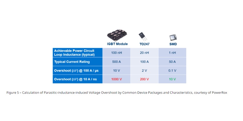
The greatly decreased switching energy and high electron mobility of a GaN HEMT compared to a Si FET can allow for transitions in the nanosecond range, but these extreme current transitions can cause previously benign parasitic loop inductances to now cause a catastrophic voltage overshoot as shown in the simple calculation examples below.

Parasitic inductances of only a mere few nanohenries may be considered negligible with current slew rates (di/dt) in Si-based designs but be catastrophic to a GaN-based design.
catastrophic effects
The equation spells out how such little ESL, from the component package alone, can have catastrophic effects on design. This is even before one has put extreme time and effort into a very clean, tight layout that contains these current flows as best as possible.
Make no mistake about it though, proper layout techniques and best practices for GaN circuits are your best weapon in the fight against EMI and hard converter failure (i.e. – self-destruction due to uncontrolled oscillation eventually building up to an electrical overstress or EOS scenario).
Gate Drive Challenges
WBG gate thresholds (Vth) tend to be lower than their Si counterparts and with lower abs. max. voltage levels, so the gate drive requirements to take advantage of GaN’s potential also have a fairly steep learning curve associated with designing and implementing such solutions robustly.
There are a variety of solutions on the market to address these challenges from integrated gate drives (or even full power stages) to fully-qualified power modules.
cross-conduction
At best, this will decrease effective efficiency and at worst will lead to the failure of the DC/DC converter
This means more care must be taken in the gate drive circuit because we have the risk of shoot-through (or false turn-on) due to high transition rates (dV/dt) acting on the switch’s gate-to-source capacitance (a.k.a. – Miller capacitance or CGS), which can apply a potential to the gate-to-drain capacitance (CGD) and trigger unwanted turn on.
If this occurs when a synchronous device is also on, then a shoot-through (a.k.a. – cross-conduction) event may occur. At best, this will decrease effective efficiency and at worst will lead to the failure of the DC/DC converter.
Challenging aspects
Different kinds of GaN can have differing gate drive requirements and this can be one of the most challenging aspects of designing with GaN components. Some can be driven direct and are normally-off devices, some use what is known as a cascade arrangement in which an enhancement-mode (i.e. – normally-off) MOSFET is used to drive the depletion-mode (i.e. – normally-on) gate of the GaN device.
Some can require negative or offset gate drive voltages. For this reason, it can be highly advantageous to acquire a qualified GaN driver, even if designing your own DC/DC solution.
Lots of Resources Out There
Users will need to go through many build and test iterations to get a truly robust, GaN-based design
There are tons of great resources out there for learning about, acquiring, and implementing GaN solutions. Some of these have already been identified above. Take advantage of them and do homework if new to WBG and GaN solutions.
Users will need to go through many build and test iterations to get a truly robust, GaN-based design, particularly for engineers newer to the space.
carefully managed layout practices
As a reminder, GaN is not a drop-in replacement for Si and therefore should not be approached as such!
The early days of investigating the use of GaN in power supplies involved a lot of people learning this lesson the hard way and even dissuading their opinion of WBG’s viability because of early failures that did not embrace the importance of carefully managed layout practices and robust gate drive design.
